SN74V293-7PZA

SN74V293-7PZA
Mfr. #:
SN74V293-7PZA
描述:
FIFO 65536 x 18 Synch FIFO Memory
生命周期:
制造商新产品。
数据表:
SN74V293-7PZA 数据表
交货:
DHL FedEx Ups TNT EMS
支付:
T/T Paypal Visa MoneyGram Western Union
ECAD Model:
更多信息:
SN74V293-7PZA 更多信息 SN74V293-7PZA Product Details
产品属性
属性值
制造商:
德州仪器
产品分类:
先进先出
RoHS:
Y
数据总线宽度:
9 bit, 18 bit
巴士方向:
单向
内存大小:
1.125 Mbit
计时类型:
同步
组织:
128 k x 9, 64 k x 18
电路数量:
2
最大时钟频率:
133 MHz
访问时间:
5 ns
电源电压 - 最大值:
3.45 V
电源电压 - 最小值:
3.15 V
电源电流 - 最大值:
35 mA
最低工作温度:
0 C
最高工作温度:
+ 70 C
包装/案例:
LQFP-80
打包:
托盘
高度:
1.4 mm
系列:
SN74V293
宽度:
14 mm
品牌:
德州仪器
安装方式:
贴片/贴片
湿气敏感:
是的
工作电源电压:
3.3 V
产品类别:
先进先出
出厂包装数量:
90
子类别:
内存和数据存储
单位重量:
0.022575 oz
Tags
SN74V29, SN74V2, SN74V, SN74, SN7
Service Guarantees

We guarantee 100% customer satisfaction.

Quality Guarantees

We provide 90-360 days warranty.

If the items you received were not in perfect quality, we would be responsible for your refund or replacement, but the items must be returned in their original condition.
Our experienced sales team and tech support team back our services to satisfy all our customers.

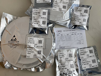
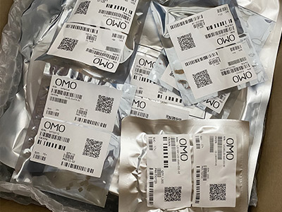
we buy and manage excess electronic components, including excess inventory identified for disposal.
Email us if you have excess stock to sell.

Email: [email protected]

Step1: Vacuum Packaging with PL
Step1:
Vacuum Packaging with PL
Step2: Anti-Static Bag
Step2:
Anti-Static Bag
Step3: Packaging Boxes
Step3:
Packaging Boxes
    A***v
    A***v
    RU

    Everything is fine. thank you very much! but very, very long delivery.

    2019-04-17
    A***a
    A***a
    RU

    Thank you!

    2019-04-13
    D***a
    D***a
    LK

    good

    2019-05-13
***roFlash
FIFO Mem Sync Dual Depth/Width Uni-Dir 64K x 18/128K x 9 80-Pin LQFP Tray
***as Instruments
65536 x 18 Synchronous FIFO Memory 80-LQFP 0 to 70
***AS INSTR
The SN74V263, SN74V273, SN74V283, and SN74V293 are exceptionally deep, high-speed, CMOS first-in first-out (FIFO) memories with clocked read and write controls and a flexible bus-matching ×9/×18 data flow.
***as Instruments Inc.
There is flexible ×9/×18 bus matching on both read and write ports.
***AS
The period required by the retransmit operation is fixed and short.
***AS INSTRUM
The first-word data-latency period, from the time the first word is written to an empty FIFO to the time it can be read, is fixed and short.
***AS INSTR
These FIFOs are particularly appropriate for network, video, telecommunications, data communications, and other applications that need to buffer large amounts of data and match buses of unequal sizes.
***
Each FIFO has a data input port (Dn) and a data output port (Qn), both of which can assume either an 18-bit or 9-bit width, as determined by the state of external control pins’ input width (IW) and output width (OW) during the master-reset cycle.
***AS INS
The input port is controlled by write-clock (WCLK) and write-enable (WEN)\ inputs. Data is written into the FIFO on every rising edge of WCLK when WEN\ is asserted. The output port is controlled by read-clock (RCLK) and read-enable (REN)\ inputs. Data is read from the FIFO on every rising edge of RCLK when REN\ is asserted. An output-enable (OE)\ input is provided for 3-state control of the outputs.
***AS INSTRUMEN
The frequencies of both the RCLK and the WCLK signals can vary from 0 to fMAX, with complete independence. There are no restrictions on the frequency of one clock input with respect to the other.
***OMO Electronic
There are two possible timing modes of operation with these devices: first-word fall-through (FWFT) mode and standard mode.
***AS INSRUMENT
In FWFT mode, the first word written to an empty FIFO is clocked directly to the data output lines after three transitions of the RCLK signal. REN\ need not be asserted for accessing the first word. However, subsequent words written to the FIFO do require a low on REN\ for access. The state of the FWFT/SI input during master reset determines the timing mode in use.
***ASIN
In standard mode, the first word written to an empty FIFO does not appear on the data output lines unless a specific read operation is performed. A read operation, which consists of activating REN\ and enabling a rising RCLK edge, shifts the word from internal memory to the data output lines.
***TEXAS
For applications requiring more data-storage capacity than a single FIFO can provide, the FWFT timing mode permits depth expansion by chaining FIFOs in series (i.e., the data outputs of one FIFO are connected to the corresponding data inputs of the next). No external logic is required.
***AS INSTUMENTS
These FIFOs have five flag pins: empty flag or output ready (EF\/OR\), full flag or input ready (FF\/IR\), half-full flag (HF)\, programmable almost-empty flag (PAE)\, and programmable almost-full flag (PAF)\. The IR\ and OR\ functions are selected in FWFT mode. The EF\ and FF\ functions are selected in standard mode. HF\, PAE\, and PAF\ always are available for use, regardless of timing mode.
***AS INSTR
PAE\ and PAF\ can be programmed independently to switch at any point in memory. Programmable offsets determine the flag-switching threshold and can be loaded by parallel or serial methods. Eight default offset settings also are provided, so that PAE\ can be set to switch at a predefined number of locations from the empty boundary. The PAF\ threshold also can be set at similar predefined values from the full boundary. The default offset values are set during master reset by the state of FSEL0, FSEL1, and LD\.
***as Instruments (TI)
For serial programming, SEN\, together with LD\, loads the offset registers via the serial input (SI) on each rising edge of WCLK. For parallel programming, WEN\, together with LD\, loads the offset registers via Dn on each rising edge of WCLK. REN\, together with LD\, can read the offsets in parallel from Qn on each rising edge of RCLK, regardless of whether serial or parallel offset loading has been selected.
***ASIN
Also, the timing modes of PAE\ and PAF\ outputs can be selected. Timing modes can be set to be either asynchronous or synchronous for PAE\ and PAF\.
***AS
If the asynchronous PAE\/PAF\ configuration is selected, PAE\ is asserted low on the low-to-high transition of RCLK. PAE\ is reset to high on the low-to-high transition of WCLK. Similarly, PAF\ is asserted low on the low-to-high transition of WCLK, and PAF\ is reset to high on the low-to-high transition of RCLK.
***XS
If the synchronous PAE\/PAF\ configuration is selected , PAE\ is asserted and updated on the rising edge of RCLK only and not WCLK. Similarly, PAF\ is asserted and updated on the rising edge of WCLK only and not RCLK. The desired mode is configured during master reset by the state of the programmable-flag mode (PFM) pin.
***AS INSTRUM
The retransmit function allows data to be reread from the FIFO more than once. A low on the RT\ input during a rising RCLK edge initiates a retransmit operation by setting the read pointer to the first location of the memory array. Zero-latency retransmit timing mode can be selected using the retransmit timing mode (RM). During master reset, a low on RM selects zero-latency retransmit. A high on RM during master reset selects normal latency.
***XS
If zero-latency retransmit operation is selected, the first data word to be retransmitted is placed on the output register with respect to the same RCLK edge that initiated the retransmit, if RT\ is low.
***AS USD
During master reset (MRS)\, the functions for all the operating modes are programmed. These include FWFT or standard timing, input bus width, output bus width, big endian or little endian, retransmit mode, programmable-flag operating and programming method, programmable-flag default offsets, and interspersed parity select. The read and write pointers are set to the first location of the FIFO. Then, based on the selected timing mode, EF\ is set low or OR\ is set high and FF\ is set high or IR\ is set low. Also, PAE\ is set low, PAF\ is set high, and HF\ is set high. The Q outputs are set low.
***AS INSTR
Partial reset (PRS)\ also sets the read and write pointers to the first location of the memory. However, the timing mode, programmable-flag programming method, default or programmed offset settings, input and output bus widths, big endian/little endian, interspersed parity select, and retransmit mode existing before partial reset is asserted remain unchanged. The flags are updated according to the timing mode and offsets in effect. PRS\ is useful for resetting a device in mid-operation when reprogramming programmable flags and other functions would be undesirable.
***AS INSTRUMENTS INC
A big-endian/little-endian data word format is provided. This function is useful when data is written into the FIFO in long-word (×18) format and read out of the FIFO in small-word (×9) format. If big-endian mode is selected, the most significant byte (MSB) (word) of the long word written into the FIFO is read out of the FIFO first, followed by the least significant byte (LSB). If little-endian format is selected, the LSB of the long word written into the FIFO is read out first, followed by the MSB. The mode desired is configured during master reset by the state of the big-endian/little-endian (BE)\ pin.
***AS INSTRUMENT
The interspersed/noninterspersed parity (IP) bit function allows the user to select the parity bit in the word loaded into the parallel port (D0–Dn) when programming the flag offsets. If interspersed-parity mode is selected, the FIFO assumes that the parity bit is located in bit position D8 during the parallel programming of the flag offsets. If noninterspersed-parity mode is selected, D8 is assumed to be a valid bit and D16 and D17 are ignored. IP mode is selected during master reset by the state of the IP input pin. This mode is relevant only when the input width is set to ×18 mode.
***AS INSTR
The SN74V263, SN74V273, SN74V283, and SN74V293 are fabricated using TI’s high-speed submicron CMOS technology.
***AS INS
For more information on this device family, see the following application reports:
型号 描述 库存 价格
SN74V293-7PZA
DISTI # V39:1801_07360563
FIFO Mem Sync Dual Depth/Width Uni-Dir 64K x 18/128K x 9 80-Pin LQFP Tray
RoHS: Compliant
0
    SN74V293-7PZA
    DISTI # 296-12492-ND
    IC SYNC FIFO MEM 65536X18 80LQFP
    RoHS: Compliant
    Min Qty: 1
    Container: Tray
    124In Stock
    • 180:$35.0906
    • 90:$38.7207
    • 10:$40.4150
    • 1:$43.3200
    SN74V293-7PZA
    DISTI # SN74V293-7PZA
    FIFO Mem Sync Dual Depth/Width Uni-Dir 64K x 18/128K x 9 80-Pin LQFP (Alt: SN74V293-7PZA)
    RoHS: Compliant
    Min Qty: 90
    Europe - 63
    • 900:€27.9900
    • 540:€29.1900
    • 360:€30.3900
    • 180:€33.3900
    • 90:€36.9900
    SN74V293-7PZA
    DISTI # SN74V293-7PZA
    FIFO Mem Sync Dual Depth/Width Uni-Dir 64K x 18/128K x 9 80-Pin LQFP - Trays (Alt: SN74V293-7PZA)
    RoHS: Not Compliant
    Min Qty: 90
    Container: Tray
    Americas - 0
    • 900:$27.7687
    • 540:$28.4543
    • 360:$29.1747
    • 180:$29.9325
    • 90:$30.3263
    SN74V293-7PZA65536 x 18 Synchronous FIFO Memory3600
    • 1000:$26.1900
    • 750:$26.2800
    • 500:$29.2700
    • 250:$31.1200
    • 100:$31.3500
    • 25:$35.2600
    • 10:$36.4200
    • 1:$38.9500
    SN74V293-7PZA
    DISTI # 595-SN74V293-7PZA
    FIFO 65536 x 18 Synch FIFO Memory
    RoHS: Compliant
    278
    • 1:$41.2500
    • 5:$40.3400
    • 10:$38.5000
    • 25:$36.8800
    • 100:$33.4200
    SN74V293-7PZAFIFO, 64KX18, 5ns, Synchronous, CMOS, PQFP80
    RoHS: Compliant
    760
    • 1000:$30.3300
    • 500:$31.9300
    • 100:$33.2400
    • 25:$34.6600
    • 1:$37.3300
    SN74V293-7PZA
    DISTI # 6625377P
    FIFO MEM SYNC DUAL DEPTH/WIDTH UNI-DIR, PU228
    • 45:£34.2800
    • 18:£35.5300
    图片 型号 描述
    MAX6365LKA31+T

    Mfr.#: MAX6365LKA31+T

    OMO.#: OMO-MAX6365LKA31-T

    Supervisory Circuits uPower Supervisor
    MAX4632CSE+

    Mfr.#: MAX4632CSE+

    OMO.#: OMO-MAX4632CSE-

    Analog Switch ICs Fault-Protected Dual Analog Switch
    MFR-25FTE52-3K

    Mfr.#: MFR-25FTE52-3K

    OMO.#: OMO-MFR-25FTE52-3K

    Metal Film Resistors - Through Hole 3K OHM 1/4W 1%
    43020-0600

    Mfr.#: 43020-0600

    OMO.#: OMO-43020-0600-410

    Headers & Wire Housings PLUG PNL MNT 6P DUAL ROW
    MFR-25FTE52-3K

    Mfr.#: MFR-25FTE52-3K

    OMO.#: OMO-MFR-25FTE52-3K-YAGEO

    Metal Film Resistors - Through Hole 3K OHM 1/4W 1%
    RMC1/16JPTP

    Mfr.#: RMC1/16JPTP

    OMO.#: OMO-RMC1-16JPTP-1190

    全新原装
    MAX4632CSE+

    Mfr.#: MAX4632CSE+

    OMO.#: OMO-MAX4632CSE--MAXIM-INTEGRATED

    IC SWITCH DUAL SPDT 16SOIC
    可用性
    库存:
    151
    订购:
    2134
    输入数量:
    SN74V293-7PZA的当前价格仅供参考,如果您想获得最优惠的价格,请提交查询或直接发送电子邮件至我们的销售团队[email protected]
    参考价格(美元)
    数量
    单价
    小计金额
    1
    US$41.25
    US$41.25
    5
    US$40.34
    US$201.70
    10
    US$38.50
    US$385.00
    25
    US$36.88
    US$922.00
    100
    US$33.42
    US$3 342.00
    250
    US$32.27
    US$8 067.50
    由于2021年半导体供不应求,低于2021年之前的正常价格,请发询价确认。
    从...开始
    最新产品
    • CC2540 Bluetooth System-on-Chip
      OMO Electronic' CC2540 is a cost-effective, low-power, true system-on-chip (SoC) for Bluetooth® low energy applications.
    • LP5907 Linear Regulator
      LP5907 linear regulators have low quiescent current and lead its class in noise performance without the use for a noise bypass capacitor.
    • CC2630/40/50 SimpleLink Wireless MCUs
      The OMO Electronic' CC2630 / CC2640 / CC2650 family of cost-effective, ultra-low power, 2.4 GHz RF devices have very-low active RF and MCU current.
    • MSP-TS430RGZ48C Target Board
      MSP-TS430RGZ48C target boards feature unified FRAM memory, enhanced MSP430 DNA, and integrated analog and digital peripherals.
    • Compare SN74V293-7PZA
      SN74V29310PZA vs SN74V29315PZA vs SN74V29315PZAG4
    • TPA3144D2 Class-D Audio Power Amplifier
      OMO Electronic' TPA3144D2 is an efficient, Class-D audio power amplifier for driving bridged-tied stereo speakers at up to 6 W, 6 Ω, or 8 Ω (per channel).
    Top